- 您现在的位置:买卖IC网 > Sheet目录1993 > DS1045S-4+T&R (Maxim Integrated Products)IC DELAY LINE 16TAP 16-SOIC
DS1045
2 of 6
PARALLEL PROGRAMMING
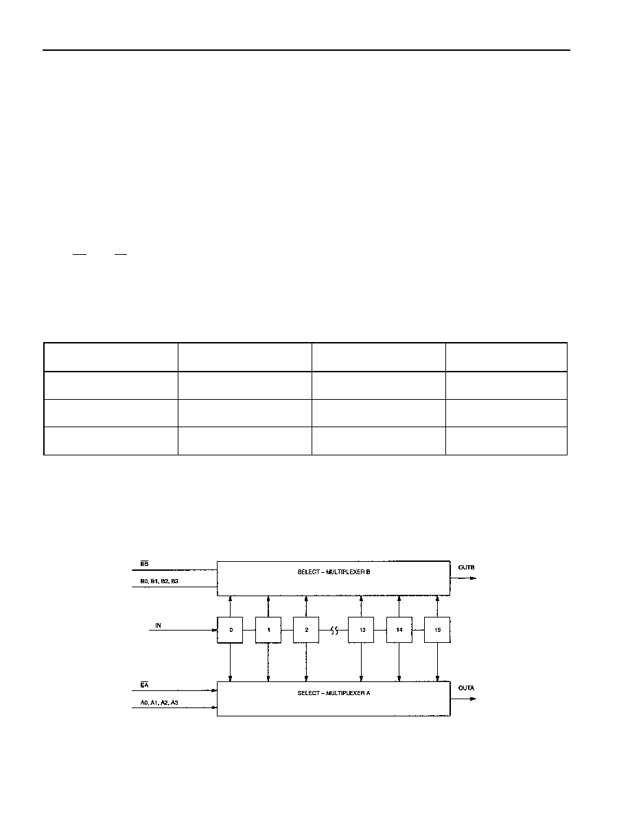
Parallel programming of the DS1045 is accomplished via the set of parallel inputs A0-A3 and B0-B3 as
shown in Figure 1. Parallel input A0-A3 and B0-B3 accept TTL levels and are used to set the delay
values of outputs OUTA and OUTB, respectively. Sixteen possible delay values between the minimum
9ns delay and the maximum delay of the DS1045-x device version can be selected using the parallel
programming inputs A0-A3 or B0-B3 (see Table 2, “Delay vs. Programmed Input”). For example, the
DS1045-3 outputs OUTA or OUTB and can be programmed to produce 16 possible delays between the
9ns (minimum) and the 54ns (maximum) in 3ns increment levels.
For applications that do not require frequent reprogramming, the parallel inputs can be set using fixed
logic levels, as would be produced by jumpers, DIP switches, or TTL levels as produced by computer
systems. Maximum flexibility in parallel programming can be achieved when inputs are set by computer-
generated data. By using the enable input pins for each respective programmed output and observing the
input setup (tDSE) and hold time (tDHE) requirements, data can be latched on an 8-bit bus. If the enable
pins, EA and EB , are not used to latch data, they should be set to a logic level 1. After each change in the
programmed delay value, a settling time (tEDV) or (tPDV) is required before the delayed output signal is
reliably produced. Since the DS1045 is a CMOS design, undefined input pins should be connected to well
defined logic levels and not left floating.
PART NUMBER TABLE Table 1
PART NUMBER
STEP ZERO DELAY
MAX DELAY TIME
MAX DELAY
TOLERANCE
DS1045-3
9
±=1ns
54ns
±2.5ns
DS1045-4
9
±=1ns
69ns
±3.3ns
DS1045-5
9
±=1ns
84ns
±4.1ns
NOTE:
Additional delay step times are available from Dallas Semiconductor by special order. Consult factory for
availability.
BLOCK DIAGRAM Figure 1
发布紧急采购,3分钟左右您将得到回复。
相关PDF资料
DS1050Z-5/T&R
IC PWM 5-BIT 5KHZ 2-WIRE 8-SOIC
DS1052Z-100+
IC PROG PWM 5BIT 100KHZ 8-SOIC
DS1077LZ-40
IC ECONOSCILLATOR 40MHZ 8-SOIC
DS1077U-120+
IC ECONOSCILLATOR 120MHZ 8-USOP
DS1081LE+
IC CLOCK MOD SS 8-TSSOP
DS1083LR-U+
IC CLOCK MOD SS 3.3V TSOT23-6
DS1100LZ-75+W
IC DELAY LINE 5TAP 75NS 8-SOIC
DS1100M-75+
IC DELAY LINE 5TAP 75NS 8-DIP
相关代理商/技术参数
DS1045S-4+W
功能描述:延迟线/计时元素
RoHS:否 制造商:Micrel 功能:Active Programmable Delay Line 传播延迟时间:1000 ps 工作温度范围: 封装 / 箱体:QFN-24 封装:Tube
DS1045S-5
功能描述:延迟线/计时元素
RoHS:否 制造商:Micrel 功能:Active Programmable Delay Line 传播延迟时间:1000 ps 工作温度范围: 封装 / 箱体:QFN-24 封装:Tube
DS1046
制造商:未知厂家 制造商全称:未知厂家 功能描述:TB motor properties
DS104C2
制造商:TOKO 制造商全称:TOKO, Inc 功能描述:Fixed Inductors for Surface Mounting
DS104LC
制造商:TOKO 制造商全称:TOKO, Inc 功能描述:Fixed Inductors for Surface Mounting
DS1050
制造商:DALLAS 制造商全称:Dallas Semiconductor 功能描述:5-Bit, Programmable, Pulse-Width Modulator: 1kHz, 5kHz, 10kHz, and 25kHz
DS1050-3
功能描述:线性和开关式电源 12V Out 1050W 1U x 2U x 11" RoHS:否 制造商:TDK-Lambda 产品:Switching Supplies 开放式框架/封闭式:Enclosed 输出功率额定值:800 W 输入电压:85 VAC to 265 VAC 输出端数量:1 输出电压(通道 1):20 V 输出电流(通道 1):40 A 商用/医用: 输出电压(通道 2): 输出电流(通道 2): 安装风格:Rack 长度: 宽度: 高度:
DS1050-3-001
制造商:Johnson Components 功能描述:AC/DC Power Supply Single-OUT 12V 87A 1.05KW 34-Pin